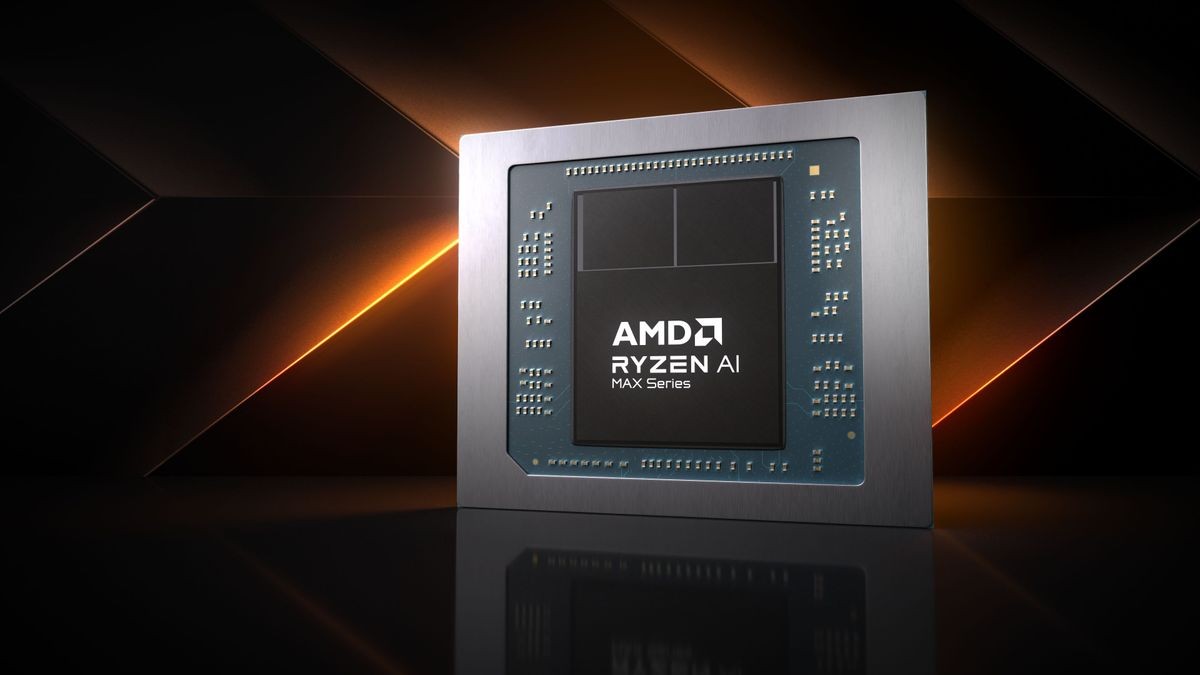
AMD has lifted the veil on its highly anticipated Strix Halo APU, now officially named Ryzen AI Max+, revealing intricate details of its innovative design through new die shots and technical annotations.
The Strix Halo represents a major leap in APU technology, featuring 16 cores and 32 threads built on the latest Zen 5 architecture, paired with a powerful 40 Compute Unit (CU) integrated GPU. The chip's architecture consists of two Zen 5 CCDs, modified from the standard Ryzen 9000 desktop versions, surrounded by eight memory ICs supporting up to 128GB of unified memory.
Recent high-resolution images showcase AMD's engineering refinements, including a 2mm reduction in Die to Die (D2D) interfaces between the CCD and I/O components. While the CCDs measure 67.07mm², they maintain 3D V-Cache compatibility, as evidenced by visible TSV connections. Each of the eight cores features 8MB of dedicated L2 cache, sharing a 32MB L3 cache pool.
The heart of the chip lies in its substantial I/O die, measuring 307.58mm². This houses a 40 CU integrated GPU based on RDNA 3.5 architecture. To address previous memory bottleneck issues, AMD implemented a dual solution: fast LPDDR5X memory across a 256-bit interface and 32MB of Memory Access at Last Level (MALL) cache split between both sides of the GPU.
A standout feature is the XDNA 2 Neural Processing Unit, which AMD claims delivers 50 TOPS of AI performance, surpassing even NVIDIA's RTX 4090. The chip also includes comprehensive connectivity options, featuring PCIe 4.0 x16, USB 4, and advanced media encoding capabilities supporting H.264, H.265, and AV1 codecs.
The complete package measures approximately 441.72mm² to 475mm², including structural silicon. The first Strix Halo-powered laptops are expected to debut this month, with Asus' ROG Flow Z13 scheduled for February 25. While initial manufacturer adoption has been cautious, market acceptance is expected to grow steadily.