NVIDIA's latest Blackwell GPU architecture faces extended testing requirements, taking three to four times longer to validate compared to its predecessor, the Hopper series. This dramatic increase in testing duration reflects the growing complexity of modern AI and data center processors.
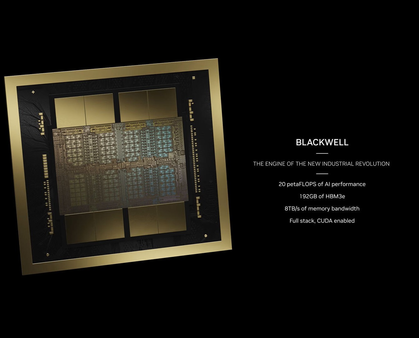
According to Advantest CEO Doug Lefever, each Blackwell GPU unit must undergo dozens of test cycles across multiple tools before it can be cleared for shipping. This intensive testing process stems from Blackwell's sophisticated design, which includes dual compute chiplets containing 104 billion transistors and eight HBM3E memory chiplets.
The testing complexity is notably higher than the previous Hopper H100 GPU, which featured a single 80-billion transistor chiplet and six HBM3 memory stacks. As transistor counts climb, testing requirements grow at an almost exponential rate, demanding more extensive test patterns and longer validation periods.
Key factors driving the extended testing time include:
- Multiple high-speed interconnects verification
- Stress condition assessments
- Thermal performance validation
- New operational modes testing, including FP4 support
- Component-level testing of compute and memory chiplets
- Package-level testing using TSMC's CoWoS-L technology
The rigorous testing protocol reflects NVIDIA's commitment to ensuring reliability and performance across various data center environments, where Blackwell GPUs must seamlessly integrate with other components like CPUs, DPUs, and network interface cards.
This development highlights the growing challenges semiconductor companies face as they push the boundaries of chip design and manufacturing complexity. The extended testing requirements, while necessary for quality assurance, add another layer of complexity to the production process of these advanced AI accelerators.