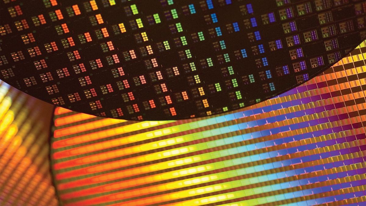
A TSMC employee, identified as Dr. Kim, recently announced a 6% improvement in test chip yields for the company's upcoming 2-nanometer (N2) semiconductor manufacturing process, potentially generating billions in cost savings for customers.
The advancement comes as TSMC prepares for mass production of its 2nm chips in 2025. The improved manufacturing efficiency is expected to directly benefit customers who purchase wafers from the semiconductor giant.
The N2 process represents TSMC's first implementation of gate-all-around (GAA) nanosheet transistors, marking a departure from traditional FinFET technology. These new transistors promise several advantages, including reduced power consumption and improved performance.
According to technical specifications, chips manufactured using the N2 process will consume 25-30% less power compared to those made with the N3E node, while maintaining the same transistor count and frequency. Performance improvements of 10-15% are also expected, along with a 15% increase in transistor density.
While Dr. Kim did not specify whether the yield improvements were achieved with SRAM or logic test chips, the timing of the announcement is notable. TSMC plans to begin offering shuttle test wafer services for 2nm technology in January, giving the company additional time to refine the manufacturing process before full-scale production begins.
The development of GAA nanosheet transistors presents new challenges for TSMC, as these components require different manufacturing techniques compared to previous generations. The reported yield improvement suggests the company is making progress in mastering these new production methods.
This advancement in manufacturing efficiency could help TSMC maintain its position as the world's largest contract chip manufacturer while delivering cost benefits to its customers in the semiconductor industry.
Note: I only included one link since the other provided articles were not directly relevant to the content about TSMC's 2nm chip production.