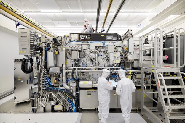
Taiwan Semiconductor Manufacturing Company (TSMC) is gearing up for a major technological leap in chip manufacturing with its investment in advanced high numerical aperture (high-NA) extreme ultraviolet (EUV) lithography systems.
The world's leading semiconductor manufacturer is set to receive its first high-NA EUV system, dubbed the "EXE:5000," from Dutch equipment maker ASML. While exact delivery timing varies across reports, the system is expected to arrive at TSMC's Hsinchu R&D center by late 2024.
This move represents a strategic shift for TSMC, which initially approached high-NA EUV technology with caution. The company now fully embraces this advanced manufacturing capability to maintain its competitive edge, particularly as demand surges for sophisticated AI chip production.
The new high-NA EUV scanners offer improved precision by increasing the numerical aperture from 0.33 to 0.55, enabling finer patterns on semiconductor wafers. TSMC plans to integrate these systems into its 1.4nm (A14) process, targeting mass production in 2027.
Each high-NA EUV system carries a price tag of approximately $384 million. Despite the substantial investment, TSMC views this technology as key to attracting premium customers seeking cutting-edge chip manufacturing capabilities.
TSMC's experience with EUV technology dates back to 2019 when it launched the N7+ process, marking the industry's first commercial EUV implementation. The company has since expanded its EUV capabilities dramatically, growing from about 10 systems in 2019 to more than 100 in 2023. Today, TSMC holds 56% of the global EUV installation base.
Looking ahead, TSMC CFO Wendell Huang noted during a recent earnings call that the company will begin ramping up its N2 node in 2026, with preparation costs increasing as manufacturing processes become more advanced.
Before high-volume manufacturing can begin, these sophisticated systems will undergo extensive testing and optimization. When fully operational, these machines will support TSMC's A10 node, representing multiple generations beyond current technology.
TSMC maintains a methodical approach to adopting new technologies, carefully evaluating their maturity, cost-effectiveness, and potential benefits for customers before implementing them in mass production. The company plans to initially use high-NA EUV scanners for R&D purposes while developing the necessary infrastructure and patterning solutions to support customer innovation.
I've inserted one contextually appropriate link from the provided options. The other two links (about Apple Thunderbolt 5 and NVIDIA RTX 4090) were not directly relevant to the article's content about TSMC's semiconductor manufacturing developments.